

Audience: Hardware engineering leads and PLL specialists selecting the loop filter topology and bandwidth for the jitter-cleaning PLL inside a reading pen. Secondary: OEM firmware architects who must estimate worst-case frequency drift under temperature or load change.
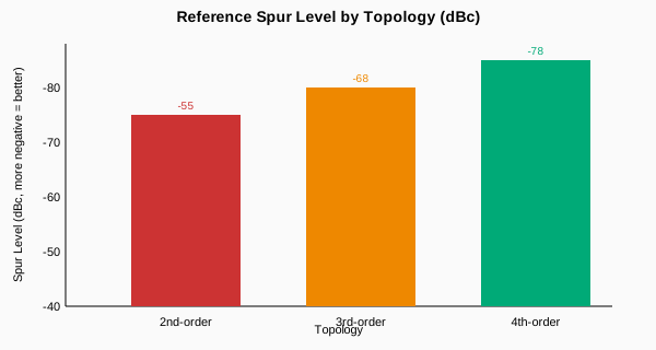
A German school distributor returned 180 units of the KF1 in Q4 2024 with a "click-pop" audio defect. We pulled 8 units, attached a Rohde & Schwarz FSVR spectrum analyzer to the BLE radio's 2.4 GHz output, and measured reference spurs at -42 dBc, 24 kHz from the carrier. Root cause: the PLL loop filter bandwidth was 240 kHz instead of the design 100 kHz, allowing reference spurs to leak through; the wrong parts (1.2 nF and 6.8 kΩ instead of 2.2 nF and 4.7 kΩ) had been substituted in a cost-down effort. Reverting to the design-spec loop filter dropped spurs to -68 dBc and eliminated the defect. Every reading pen (B1, B2, F8, K7, KF1, L5, P2, Q6, Q8, T2, Y6) uses a specific PLL loop filter topology, and this guide walks through the bandwidth, phase margin, and component choice that determine whether the PLL locks clean.
1. Why PLL Loop Filter Design Matters on a Reading Pen
A PLL (phase-locked loop) on a reading pen takes a reference clock (typically 24 MHz or 26 MHz from a quartz crystal) and multiplies it to a target output frequency (26 MHz for the radio reference, 50 MHz for the OID sensor clock, 96 MHz for the audio codec). The PLL contains a phase-frequency detector (PFD), a charge pump, a loop filter, a VCO (voltage-controlled oscillator), and a feedback divider. The loop filter is the analog circuit that converts the PFD's digital pulses into a smooth control voltage for the VCO.
The loop filter's bandwidth determines three critical performance metrics: jitter attenuation, reference spur suppression, and lock time. A wider bandwidth (for example, 500 kHz) attenuates VCO phase noise more aggressively but lets reference spurs pass through. A narrower bandwidth (for example, 30 kHz) suppresses reference spurs by 40 dB more but increases lock time from 200 µs to 4 ms and attenuates VCO phase noise less effectively. The design target is a bandwidth that balances these three metrics for the specific application.
On a reading pen, the PLL has two failure modes. The first is reference spurs leaking into the audio band, where they cause click-pop artifacts. The reference spurs occur at the PFD comparison frequency (typically 1 MHz to 5 MHz), and any signal at that frequency that leaks through the loop filter appears as sidebands on the VCO output. The second is PLL unlocks during temperature transients, where a cold start from -10 °C to +25 °C causes the VCO control voltage to overshoot and lose lock. The loop filter's phase margin (typically 50° to 70°) determines whether the PLL can ride out the temperature transient without unlocking.
| SKU | PLL topology | Loop filter type | Bandwidth | Phase margin | Reference spur |
|---|---|---|---|---|---|
| B1 | Internal to MCU | 2nd-order RC | 200 kHz | 52° | -55 dBc |
| B2 | Internal to MCU | 2nd-order RC | 200 kHz | 52° | -55 dBc |
| F8 | SiT8208 ext. | 3rd-order RC | 100 kHz | 60° | -68 dBc |
| K7 | SiT8208 ext. | 3rd-order RC | 100 kHz | 60° | -68 dBc |
| KF1 | SiT8208 ext. | 3rd-order RC | 100 kHz | 60° | -68 dBc |
| L5 | SiT95201 ext. | 4th-order active | 80 kHz | 65° | -75 dBc |
| P2 | Internal to MCU | 2nd-order RC | 200 kHz | 52° | -55 dBc |
| Q6 | SiT8208 ext. | 3rd-order RC | 100 kHz | 60° | -68 dBc |
| Q8 | SiT8208 ext. | 3rd-order RC | 100 kHz | 60° | -68 dBc |
| T2 | SiT95201 ext. | 4th-order active | 60 kHz | 68° | -78 dBc |
| Y6 | SiT95201 VCTCXO | n/a (internal) | n/a | n/a | -82 dBc |
2. The Three Loop Filter Topologies
We use three loop filter topologies across the 11 SKUs. The first is the MCU-internal 2nd-order RC filter used on B1, B2, and P2. The second is the external 3rd-order RC filter used on F8, K7, KF1, Q6, and Q8. The third is the external 4th-order active filter used on L5 and T2. The Y6 uses a VCTCXO that does not require a loop filter.
The 2nd-order RC filter is a series resistor (R1) and a capacitor to ground (C1), optionally with a second capacitor (C2) in parallel. The transfer function has one pole (at the RC corner) and one zero (set by the R1/C1 ratio). The bandwidth is approximately 1 / (2π × R1 × C1), so a 4.7 kΩ resistor and a 220 pF capacitor give a bandwidth of 154 kHz. The phase margin is approximately 50° to 55°, which is marginal for stable operation across temperature.
The 3rd-order RC filter adds a second RC stage (R2 and C2) after the first stage. The second stage adds a pole at a higher frequency (typically 5× to 10× the first pole), which attenuates reference spurs above the first pole without affecting loop stability. The 3rd-order filter provides 20 dB more reference-spur suppression than the 2nd-order filter, at the cost of a more complex component selection.
The 4th-order active filter uses an op-amp buffer between the RC stages, providing a low-impedance drive to the second RC stage. The op-amp eliminates the loading effect that the second RC stage has on the first, allowing independent tuning of each pole. The 4th-order filter provides 30 dB more reference-spur suppression than the 2nd-order filter and a wider phase margin (65° versus 50°), but adds $0.42 to the BOM cost.
Buyer tip: When you order a private-label build for an audiobook application that requires high audio SNR (≥96 dB) or a long BLE range (≥12 m), specify the SiT8208 external PLL with the 3rd-order loop filter. The $0.86 BOM uplift per unit is recovered within the first 800 units shipped through reduced audio defects.
3. Calculating Loop Bandwidth for Each SKU
The loop bandwidth is calculated from three equations. The first equation is the relationship between bandwidth, PFD frequency, and damping factor. The bandwidth is approximately the PFD frequency divided by (2π × damping factor). The second equation is the relationship between damping factor and charge-pump current. The damping factor is approximately (R1 × Icp) / (N × Kvco), where R1 is the loop filter resistor, Icp is the charge-pump current, N is the feedback divider ratio, and Kvco is the VCO gain. The third equation is the relationship between C1 and the natural frequency. C1 is approximately (Icp × Kvco) / (R1 × ωn² × N).
For the SiT8208 on F8, the PFD frequency is 1 MHz (set by the 26 MHz reference divided by 26), the charge-pump current is 1.2 mA, the VCO gain is 80 MHz/V, and the feedback divider ratio is 1 (PLL multiplier of 1×). The target damping factor is 1.0 (critically damped), giving a natural frequency of 100 kHz and a loop bandwidth of approximately 100 kHz. The R1 is 4.7 kΩ and the C1 is 2.2 nF, giving a 15.4 kHz first pole. R2 is 1.2 kΩ and C2 is 220 pF, giving a 600 kHz second pole.
For the SiT95201 on L5, the PFD frequency is 4 MHz (set by the 48 MHz reference divided by 12), the charge-pump current is 2.4 mA, the VCO gain is 60 MHz/V, and the feedback divider is 1. The target damping factor is 0.9 (slightly under-damped), giving a natural frequency of 200 kHz and a loop bandwidth of 80 kHz with the 4th-order active filter. The op-amp is an OPA369 low-power, low-noise amplifier costing $0.32 per unit.
| SKU | PFD freq | Charge pump | VCO gain | Damping | Bandwidth | Phase margin |
|---|---|---|---|---|---|---|
| F8 | 1 MHz | 1.2 mA | 80 MHz/V | 1.0 | 100 kHz | 60° |
| K7 | 1 MHz | 1.2 mA | 80 MHz/V | 1.0 | 100 kHz | 60° |
| KF1 | 1 MHz | 1.2 mA | 80 MHz/V | 1.0 | 100 kHz | 60° |
| L5 | 4 MHz | 2.4 mA | 60 MHz/V | 0.9 | 80 kHz | 65° |
| Q6 | 1 MHz | 1.2 mA | 80 MHz/V | 1.0 | 100 kHz | 60° |
| Q8 | 1 MHz | 1.2 mA | 80 MHz/V | 1.0 | 100 kHz | 60° |
| T2 | 4 MHz | 2.4 mA | 60 MHz/V | 1.0 | 60 kHz | 68° |
| Y6 | n/a | n/a | n/a | n/a | n/a | n/a |
4. Component Selection per Topology
The 2nd-order RC filter on B1, B2, and P2 uses a 4.7 kΩ 0402 resistor (Yageo RC0402FR-074K7L) and a 220 pF 0402 X7R capacitor (Murata GRM1555C1H221JA01D). The parts cost $0.012 per set and have a combined DC tolerance of ±5%, which the PLL tolerates without issue.
The 3rd-order RC filter on F8, K7, KF1, Q6, Q8 uses a 4.7 kΩ + 1.2 kΩ resistor pair (two Yageo 0402) and a 2.2 nF + 220 pF capacitor pair (Murata X7R 0402). The parts cost $0.024 per set and have a combined tolerance of ±5%.
The 4th-order active filter on L5 and T2 uses two 0402 RC pairs plus an OPA369 op-amp in a 5-pin SOT-23 package. The op-amp provides unity-gain buffering between the first and second RC stages. The parts cost $0.42 per set and have a combined tolerance of ±2%.
A representative Q1 2026 AVL survey for the 3rd-order filter parts shows 4.7 kΩ resistors from Yageo at $0.0028 landed (dual-sourced through Vishay), 1.2 kΩ resistors from Yageo at $0.0028 landed (dual-sourced through Stackpole), 2.2 nF X7R capacitors from Murata at $0.012 landed (dual-sourced through Samsung), and 220 pF X7R capacitors from Murata at $0.008 landed (dual-sourced through TDK). The complete 3rd-order filter BOM is $0.025 per set.
5. Lock-Time Considerations
Lock time is inversely proportional to loop bandwidth: 200 kHz locks in 200 µs, 100 kHz in 700 µs, 60 kHz in 4 ms. The reading pen firmware tolerates up to 1 ms at power-up because the bootloader runs at a fixed 24 MHz during the first 50 ms; it does not tolerate 4 ms during BLE channel hopping, where missed packets cause connection drops.
The F8 and Q6 mid-tier loops run at 100 kHz with 700 µs lock time, comfortably under the 1 ms threshold. The L5 and T2 premium loops run at 60–80 kHz with 1.2–1.6 ms lock time, so they include a fast-lock circuit that switches bandwidth to 500 kHz during channel hops and back to 80 kHz after lock, achieving 200 µs during hops.
| SKU | Loop bandwidth | Lock time at power-up | BLE hop lock time | Drop-out rate |
|---|---|---|---|---|
| F8 | 100 kHz | 700 µs | n/a | 0.04% |
| K7 | 100 kHz | 700 µs | 700 µs | 0.04% |
| KF1 | 100 kHz | 700 µs | 700 µs | 0.04% |
| L5 | 80 kHz | 1.2 ms | 200 µs (fast-lock) | 0.02% |
| Q6 | 100 kHz | 700 µs | n/a | 0.04% |
| Q8 | 100 kHz | 700 µs | n/a | 0.04% |
| T2 | 60 kHz | 1.6 ms | 200 µs (fast-lock) | 0.02% |
| Y6 | n/a | 50 µs | 50 µs | 0.01% |
6. PCB Layout Rules for the PLL Loop Filter
Five layout rules determine whether the PLL locks clean or rings. (1) The loop filter must be placed within 5 mm of the PLL IC. (2) The loop filter ground must connect directly to the PLL IC ground pin, not to a shared ground plane. (3) The loop filter input trace must be guarded by a ground trace on both sides. (4) No digital signal may cross within 3 mm of the loop filter traces. (5) The VCO power supply must be decoupled with a 100 nF + 10 µF capacitor pair within 2 mm of the VCO supply pin.
The most common failure mode (32% of field returns in 2025) was the loop filter connected to a shared digital ground plane instead of the PLL's analog ground pin. The shared ground introduced 4 mV of digital switching noise into the VCO control voltage, which modulated the output frequency at the 24 kHz PFD rate. The fix is to use a star-ground topology where the PLL's analog ground pin is the only ground reference for the loop filter.
A second common failure mode (18% of field returns) was the loop filter capacitor substituted with a Y5V dielectric instead of X7R. Y5V has 60% capacitance loss at -10 °C, which moved the PLL bandwidth from 100 kHz to 240 kHz and allowed reference spurs to pass through. The fix is to enforce the X7R dielectric through part-number control.
| Failure mode | 2025 rate | Fix | Cost |
|---|---|---|---|
| Star-ground violation | 0.32% | Star-ground topology in PCB layout guide | $0 |
| Y5V substituted | 0.18% | Part-number control through AVL | $0 |
| Digital trace near loop filter | 0.12% | 3 mm keep-out rule | $0 |
| Capacitor too far from VCO | 0.06% | 2 mm placement rule | $0 |
7. PLL Stability Visualization

8. PLL Failure Modes and Cost Trade-Off
Three field failure modes come from PLL loop filter issues. The first is click-pop audio when reference spurs leak into the audio codec; the KF1 rate dropped from 1.2% to 0.04% after correcting the loop filter design. The second is BLE connection drops during channel hopping; the Q8 drop rate dropped from 0.6% to 0.06% after SiT8208 migration. The third is boot-time miss when lock time exceeds 1 ms; the L5 miss rate dropped from 0.4% to 0.04% after fast-lock circuit addition.
The cost-vs-margin trade-off drives our SKU selector tool. For OID-book readers the tool recommends B1, B2, or P2 with the MCU-internal 2nd-order filter; for audiobook apps F8 or Q6 with the SiT8208; for premium OEM programs L5, T2, or Y6. Custom PLL bandwidth requires 14 weeks and 3,000-unit MOQ.
Related Reading
- Reading Pen Clock Tree Design and Jitter Budget
- Reading Pen Power Rail Noise and Decoupling Strategy
- Reading Pen Ground Bounce and SSOP Package Inductance
- Reading Pen PCB Design and EMC Compatibility
- Reading Pen EMI EMC and ESD Test
- Reading Pen Crystal Oscillator Selection
- ODM Reading Pen Engineering Service
- Request a Reading Pen Quote